


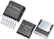
Infineon Technologies CoolSiC ™ 650V G2碳化矽MOSFET
英飛凌CoolSiC™ 650V G2碳化矽MOSFET利用碳化矽的性能優勢,通過降低能量損耗來提高功率轉換過程中的效率,這為光伏、儲能、直流電動車充電、馬達驅動和工業電源等各種功率半導體應用提供了優勢。配備CoolSiC G2的電動車直流快速充電站,可比前一代產品減少10%的功率損耗,同時在不影響外形尺寸的情況下實現更高的充電容量。
特點
- 靈活的驅動電壓,並與雙極驅動方案相容
- 基準閘極臨界電壓VGS(th) = 4.5V
- 即使關斷閘極電壓為0V,仍可穩健地防止寄生導通
- 靈活的驅動電壓,與雙極驅動方案相容
- 超低開關損耗
- 堅固的體二極體可在硬換向事件下工作
- .XT互連技術提供優異的散熱性能
應用
- SMPS
- 太陽能PV逆變器
- 能量儲存與電池組成
- UPS
- 電動車充電基礎設施
- 馬達驅動器

影片

相關產品

Infineon Technologies CoolSiC™ G2碳化矽MOSFET
在AC-DC、DC-DC和DC-AC應用中達到最高品質標準的同時,實現優異的SiC性能水準。
Infineon Technologies CoolSiC™ 400V G2 Silicon Carbide MOSFETs
Specially developed for use in the AC/DC stage of AI server PSUs and solar/energy storage systems.

Infineon Technologies CoolSiC™ MOSFETs 650V
Combines the strength of silicon carbide with device performance, reliability, and ease of use.

Infineon Technologies CoolSiC™ 1200V G2碳化矽MOSFET
用於電力電子應用的高性能解決方案。
Development Tools

Infineon Technologies EVAL-2KW-SIC-IH Eval Board for Induction Heating
Designed to showcase the CoolSiC™ 650V G2 MOSFET family for induction heating applications.

Infineon Technologies EVAL_5K5W_3PH_LLC_SIC2 Interleaved LLC Converter
An interleaved LLC converter that converts a 400VDC input voltage to a regulated 50V output.

Infineon Technologies REF-10KW-3LBUCK-SIC400 Reference Board
Enables evaluation of CoolSiC™ MOSFET 400V/650V G2 in TOLL and D2PAK-7 packages.