Toshiba TC7WP3125FK & TC7WP3125FC Integrated Circuits
Toshiba TC7WP3125FK and TC7WP3125FC Integrated Circuits are dual-supply, advanced high-speed CMOS 2-bit dual-supply voltage interface bus buffers fabricated with silicon gate CMOS technology. The Toshiba TC7WP3125FK and TC7WP3125FC are designed with over-voltage-tolerant inputs and outputs up to 3.6V.Features
- Level converter for interfacing 1.2V to 1.8V, 1.2V to 2.5V, 1.2V to 3.3V, 1.5V to 2.5V, 1.5V to 3.3V, 1.8V to 2.5V, 1.8V to 3.3V or 2.5V to 3.3V system
- High-speed operation
- tpd = 6.8ns (max) (VCCA = 2.5 ± 0.2V, VCCB = 3.3 ± 0.3V)
- tpd = 7.8ns (max) (VCCA = 1.8 ± 0.15V, VCCB = 3.3 ± 0.3V)
- tpd = 8.6ns (max) (VCCA = 1.5 ± 0.1V, VCCB = 3.3 ± 0.3V)
- tpd = 22ns (max) (VCCA = 1.2 ± 0.1V, VCCB = 3.3 ± 0.3V)
- tpd = 9.5ns (max) (VCCA = 1.8 ± 0.15V, VCCB = 2.5 ± 0.2V)
- tpd = 10.8ns (max) (VCCA = 1.5 ± 0.15V, VCCB = 2.5 ± 0.2V)
- tpd = 23ns (max) (VCCA = 1.2 ± 0.15V, VCCB = 2.5 ± 0.2V)
- tpd = 30ns (max) (VCCA = 1.2 ± 0.1V, VCCB = 1.8 ± 0.15V)
- Output current
- |IOHB|/IOLB = 3 mA (min) (VCCB = 3.0 V)
- |IOHB|/IOLB = 2 mA (min) (VCCB = 2.3 V)
- |IOHB|/IOLB = 0.5 mA (min) (VCCB = 1.65 V)
- Latch-up performance of -300mA
- ESD performance
- Machine model ≥ ±200V
- Human body model ≥ ±2000V
- Ultra-small package of CSON8 (CST8) or SSOP8 (US8)
- Low current consumption
- Using the new circuit significantly reduces current consumption when OE = “H”
- Suitable for battery-driven applications such as PDAs and cellular phones
- 3.6V tolerant function and power-down protection provided on all inputs and outputs
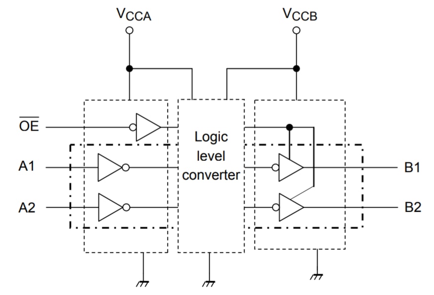
Block Diagram

發佈日期: 2020-10-14
| 更新日期: 2024-11-25


