


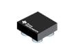
Texas Instruments TPS22968/Q1 Dual Channel Load Switch
Texas Instruments TPS22968/Q1 Dual Channel Load Switch is a small, ultra-low RON, dual channel load switch with controlled turn on. The device contains two N-channel MOSFETs that can operate over an input voltage range of 0.8V to 5.5V and can support a maximum continuous current of 4A per channel. Each switch is independently controlled by an on/off input (ON1 and ON2), which is capable of interfacing directly with low-voltage control signals. In TPS22968, a 270Ω on-chip load resistor is added for output quick discharge when switch is turned off. The TPS22968 is available in a small, space-saving package (DPU) with integrated thermal pad allowing for high power dissipation. The device is characterized for operation over the free-air temperature range of -40 to 85°C. The TPS22968-Q1 devices are AEC-Q100 qualified for automotive applications.
Features
- Integrated dual channel load switch
- 0.8V to 5.5V Input voltage range
- 2.5V to 5.5V Ideal for 1S battery configuration VBIAS voltage range
- Ultra low RON resistance RON = 27mΩ at VIN = 5V (VBIAS = 5V)
- RON = 25mΩ at VIN = 3.3V (VBIAS = 5V)
- RON = 25mΩ at VIN = 1.8V (VBIAS = 5V)
- 4A Maximum continuous switch current per channel
- Low quiescent current 55µA at VBIAS = 5V (both channels)
- 55µA at VBIAS = 5V (Single channel)
- Low control input threshold enables use of 1.2V/1.8V/2.5V/3.3V logic
- Configurable rise time
- Quick Output Discharge (QOD)
- SON 14-pin package with thermal pad
- ESD Performance tested per JEDEC STD2KV HBM and 1KV CDM
- Latch-up performance exceeds 100mA Per JESD 78, class II
- GPIO Enable - active high
Applications
- Ultrabook™
- Notebooks/netbooks
- Tablets
- Consumer electronics
- Set-top boxes
- Telecom systems
Development Tools
Texas Instruments TPS22968NEVM Dual Channel Load Switch EVMs
Evaluates the TPS22968N, a dual channel load switch with an operating voltage of 0.8V to 5.5V.

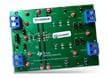
Texas Instruments TPS22968Q1 Dual Channel Automotive Load Switch EVM
Designed to demonstrate the features of the TPS22968-Q1 a dual switch ultra low Ron device.
Related Products
Texas Instruments TPS229xx Load Switches
Small, low on-resistance, single channel load switches with a controlled slew rate.
Functional Block Diagram

發佈日期: 2015-03-11
| 更新日期: 2022-03-11