


Lattice Semiconductor MachXO4™ Field-Programmable Gate Arrays

Lattice Semiconductor MachXO4™ Field-Programmable Gate Arrays (FPGAs) expand Lattice Semiconductor’s ultra-low-density FPGA portfolio with advanced features that deliver flexibility and efficiency. The MachXO4 devices combine low power consumption, embedded flash, high I/O density, and instant-on capability to meet the needs of modern systems. With exceptional I/O density in compact packages, MachXO4 integrates hardened functions that help minimize system cost and footprint. Broad programmability and native support for industry-standard interfaces make these FPGAs a scalable solution for evolving connectivity and control applications.
Design productivity is enhanced through Lattice Radiant™ software, which supports large and complex designs with industry-leading RTL synthesis, a unified design database, advanced scripting, a modern GUI, timing analysis, and an embedded logic analyzer. Lattice also offers a wide range of pre-engineered IP modules for the MachXO4™ family.
Features
- Variants (All functionally and pin-compatible)
- ZC - ultra-low-power, 2.5V/3.3V supply
- HC - high-performance, 2.5V/3.3V supply
- HE - high-performance, 1.2V supply
- Built on a 65nm non-volatile, low-power process
- Extremely low power consumption, as low as 140µW of static power
- Wide 896 LUTs to 9400 LUTs logic density selection range
- Embedded flash memory with User Flash Memory (UFM) of up to 448kb
- Up to 432kb of Embedded Block Memory (EBR) and 54kb of Distributed RAM
- Instant-on power-up with fast boot time of less than 5ms
- Highly flexible buffer supporting 3.3V, 1V I/O standards for interfacing legacy and next-generation devices
- Hot socketing with leakage current as low as 350µA and no power supply sequencing
- Mixed voltage support for LVCMOS and LVTTL I/O types
- Default integrated pull-down resistors to minimize external components
- Compact packages with a high I/O-to-LUT ratio, up to 382x I/O pins
- SPI, I2C, timer/counter, and oscillator on-chip hardened functions
- Improved design productivity using Lattice Radiant Software
- RoHS compliant
Applications
- Compute
- Data center servers
- Networking and storage
- Hardware acceleration
- Communications
- Ethernet switches and routers
- Broadband access
- Radio units
- Consumer electronics
- Display monitors
- Cameras
- Smart phones
- Industrial
- Motor control
- Handheld devices
- Test and measurement
- Programmable logic controllers
- Automotive (parts ending in A)
- ADAS
- Inverters
- Motor control
- Infotainment
- Battery management
Specifications
- Low-power and programmable architecture
- Logic density ranging from 896 to 9.4k LUT4
- 64kb to 432kb of Embedded Block Memory (EBR)
- Up to 54kb of distributed RAM
- Dedicated FIFO control logic
- Advanced 65nm low-power process
- Programmable low swing differential I/O
- Stand-by mode and other power-saving options
- High-performance, flexible I/O buffer
- Programmable sysI/O™ buffer supports a wide range of interfaces
- LVCMOS 3.3/2.5/1.8/1.5/1.2/1.0
- LVTTL
- LVDS, Bus-LVDS, MLVDS, LVPECL
- MIPI D-PHY emulated
- Schmitt trigger inputs, up to 0.5V hysteresis
- I/O support hot socketing
- On-chip differential termination
- Programmable pull-up or pull-down mode
- Programmable sysI/O™ buffer supports a wide range of interfaces
- Pre-engineered source synchronous I/O
- DDR registers in I/O cells
- Dedicated gearing logic
- 7:1 gearing for display I/O
- Generic DDR, DDRx2, and DDRx4
- Broad range of advanced packaging
- Compact packages with a high I/O-to-LUT ratio up to 382 I/O pins
- 0.4mm pitch - 1280 to 4320 LUTs in a very small footprint WLCSP (2.5mm × 2.5mm to 3.8mm × 3.8mm) with 27 to 62 I/Os
- 0.5mm pitch - 896 to 4320 LUTs in 8mm x 8mm BGA to 20mm x 20mm TQFP packages with up to 112 I/Os
- 0.8mm pitch - 1280 to 9400 LUTs in 14mm x 14mm to 19mm x 19mm BGA packages with up to 382 I/Os
- 1.0mm pitch - 1280 to 4320 LUTs in a 17mm x 17mm BGA package with 204 I/Os
- Non-volatile, multi-time reconfigurable
- Instant-on - powers up in milliseconds
- Optional dual boot with external SPI memory
- Single-chip, secure solution
- Programmable through JTAG, SPI, or I2C
- Reconfigurable Flash up to 100,000 write/erase cycles for commercial/industrial devices and 10,000 write/erase cycles for automotive devices
- Supports background programming of non-volatile memory
- In-field logic update while I/O holds the system state through TransFR reconfiguration
- Optimizable on-chip clocking
- On-chip oscillator with 5.5% accuracy for commercial/industrial devices
- 8 primary clocks
- Up to two edge clocks for high-speed I/O interfaces, top and bottom sides only
- Up to two analog PLLs per device with fractional-n frequency synthesis
- Wide 7MHz to 400MHz input frequency range
- Enhanced system-level support
- On-chip hardened functions - SPI, I2C, and timer/counter
- Unique TraceID for system tracking
- Single power supply with extended operating range
- IEEE Standard 1149.1 boundary scan
- IEEE 1532-compliant in-system programming
- State-of-the-art design software
- MachXO4 device is supported in Lattice Radiant
- Industry-leading RTL language support for VHDL, VHDL-2008, Verilog, and SystemVerilog
- Advanced scripting capability on the command-line and TCL design flow
- One-click compilation flow and cross-probing between analysis tools
- Embedded timing and logic analyzer
PFU Block Diagram

The core of the MachXO4 device consists of PFU blocks, which can be programmed to perform logic, arithmetic, distributed RAM, and distributed ROM functions. Each PFU block consists of four interconnected slices numbered zero to three. Each slice contains two LUTs and two registers. There are 53 inputs and 25 outputs associated with each PFU block.
Slice Diagram

Slices zero to three contain two LUT4s feeding two registers. Slices zero to two can be configured as distributed memory. The control logic performs set/reset functions (programmable as synchronous/ asynchronous), clock select, chip select, and wider RAM/ROM functions. The registers in the slice can be configured for positive/negative and edge-triggered or level-sensitive clocks. All slices have 15 inputs from routing and one from the carry-chain (from the adjacent slice or PFU). There are seven outputs: six for routing and one to carry-chain (to the adjacent PFU).
PLL Diagram

The MachXO4 PLL contains a WISHBONE port feature that allows the PLL settings, including divider values, to be dynamically changed from the user logic. When using this feature, the EFB block must also be instantiated in the design to allow access to the WISHBONE ports. Similar to the dynamic phase adjustment, when PLL settings are updated through the WISHBONE port, the PLL may lose lock and not relock until the tLOCK parameter has been satisfied.
Devvelopment Tool
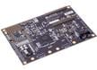
Lattice Semiconductor MachXO4™ Development Board
Versatile platform for exploring and evaluating the capabilities of the MachXO4 FPGA.