Texas Instruments SN74ACT2G100/SN74ACT2G100-Q1 Flip-Flops
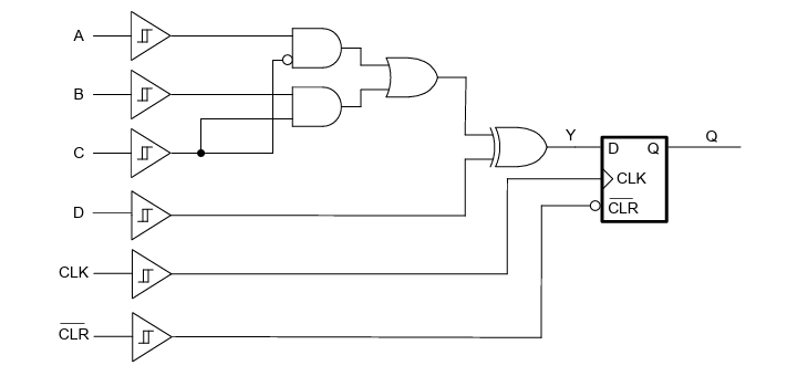
Texas Instruments SN74ACT2G100/SN74ACT2G100-Q1 Flip-Flops contain two independent D-type flip-flops with rising-edge-triggered clock, active-low clear, and configurable logic data inputs. The data inputs can be configured for multiple 1- and 2-input logic functions, including buffer, inverter, AND, OR, NAND, NOR, XOR, and XNOR. All inputs on the TI SN74ACT2G100/SN74ACT2G100-Q1 Flip-Flops have a Schmitt-trigger architecture to support slow or noisy input signals.
The SN74ACT2G100-Q1 devices are AEC-Q100 qualified for automotive applications.
Features
- AEC-Q100 qualified for automotive applications:
- Device temperature grade 1: -40° to +125°
- Device HBM ESD classification level 2
- Device CDM ESD classification level C4B
- Available in a wettable flank QFN package
- Operating voltage range of 4.5V to 5.5V
- TTL-compatible Schmitt-trigger inputs support slow and noisy input signals
- Continuous ±24mA output drive at 5V
- Supports up to ±75mA output drive at 5V in short bursts
- Drives 50Q transmission lines
- Fast operation with a delay of 10.4ns max
Applications
- Hold a signal during controller reset
- Input slow edge-rate signals
- Operate in noisy environments
Datasheets
Logic Diagram (Positive Logic)

發佈日期: 2026-01-06
| 更新日期: 2026-01-12


