


NXP Semiconductors VR5510 Multi-Output PMICs
NXP Semiconductors VR5510 Automotive Multi-Output PMICs are designed for Gateway, ADAS, V2X, and infotainment applications. The VR5510 includes multiple high-efficiency switch modes and linear voltage regulators. The PMICs provide external frequency synchronization on inputs and outputs for optimized system EMC performance.
The NXP Semiconductors VR5510 Automotive Multi-Output PMICs have enhanced safety features with fail-safe outputs and covers ASIL B and ASIL D safety integrity levels. The VR5510 can be fully implemented in a safety-oriented system partitioning and can also be configured to operate as a non-safety QM-version part.
The VR5510 is available in several versions that support various safety applications and present numerous choices for the number of output rails, output voltage settings, operating frequencies, and power-up sequencing.
The VR551 if offered in QFN56 package with thermally enhanced wettable flanks. Devices with wettable flanks enable Automated Optical Inspection (AOI), exhibit a greater resistance to shear forces, and can handle PCB flexing, thus improving reliability.
Features
- 60VDC maximum input voltage
- VPRE synchronous buck controller with external MOSFETs
- Configurable output voltage, switching frequency, and current capability up to 10A
- Low-voltage integrated synchronous BUCK1 and BUCK2 converters dedicated to MCU core supply with SVS/DVS capability
- Configurable output voltage and current capability up to 3.6A peak; Dual-phase operation to extend the current capability up to 7.2A peak
- Low-voltage integrated synchronous BUCK3 converter
- Configurable output voltage and current capability up to 3.6A peak
- BOOST converter with integrated low-side switch
- Configurable output voltage and input current capability up to 2.25A peak
- 3x linear voltage regulators (LDOx) for MCU IOs, DDR and ADC supplies
- Configurable output voltage and current capability up to 400mA
- High-voltage linear regulator (HVLDO) with current capability up to 10mA in LDO mode and 100mA in switch mode
- EMC optimization techniques, including SMPS frequency synchronization, spread spectrum, slew rate control, manual frequency tuning
- Low-power standby mode with very low quiescent current (35μA with VPRE and HVLDO ON)
- 2x input pins for wake-up detection and battery voltage sense
- Device control via I2C interface with CRC (up to 3.4MHz)
- Dual device operation possible via dedicated synchronization pin
- Scalable portfolio from QM to ASIL B to ASIL D with independent monitoring circuitry, dedicated interface for MCU monitoring, simple and challenger watchdog function, power good, reset and interrupt, built-in self-test, fail-safe output
- Configuration by OTP programming
- Prototype enablement to support custom setting during project development in engineering mode
- 8.0mm x 8.0mm x 0.85 QFN56 package; 0.5mm pitch
Applications
- Gateway
- Infotainment
- ADAS
- Clusters
- V2x
- Radio
- Vision
Associated Products
NXP Semiconductors S32G3車輛網路處理器
結合了CAN、LIN和FlexRay網路,以及高資料傳輸速率的乙太網路連網功能。
NXP Semiconductors VR5510 Multi-Output PMICs
Automotive Multi-Output PMICs designed for Gateway, ADAS, V2X, and infotainment applications.
Development Tools
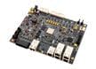
NXP Semiconductors S32G Reference Design 2 (S32G-VNP-RDB2)
Highly-optimized evaluation board based on the S32G2 Vehicle Network Processor.
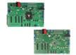
NXP Semiconductors KITVR5510xA0EVM Evaluation Boards
Allow access to all features and functions of the VR5510 PMICs.
NXP Semiconductors GoldBox 3 Vehicle Networking Development Platform
Designed for vehicle SoGs, domain control, and safety/security applications.

NXP Semiconductors SJA1110-MGS-EVM Evaluation Board
Compact, cost-effective multi-gig secure evaluation board, ideal for automotive Ethernet use cases.
Simplified Application Diagram

Internal Block Diagram

Package Outline
