


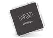
NXP Semiconductors LPC55S1x/LPC551x Microcontrollers (MCUs)
NXP Semiconductors LPC55S1x and LPC551x Microcontrollers (MCUs) are 32-bit Arm® Cortex®-M33 based modules designed for general-purpose embedded applications. The Arm Cortex-M33 CPU architecture features 150MHz frequency and provides a security foundation with isolation to protect valuable IP and data with TrustZone® technology. This simplifies the design and software development of digital signal control systems with integrated digital signal processing (DSP) instructions. NXP LPC55S1x and LPC551x MCUs also offer support for secure boot, HASH, AES, RSA, UUID, dynamic encrypt and decrypt, debug authentication, and TBSA compliance. Typical applications include industrial IoT, industrial automation, building control, diagnostic equipment, and consumer electronics.
Features
- Arm Cortex-M33 core
- Running at frequency of up to 150MHz
- TrustZone, floating point unit (FPU), and memory protection unit (MPU)
- Arm Cortex-M33 built-in nested vectored interrupt controller (NVIC)
- Non-maskable interrupt (NMI) input with selection of sources
- Serial wire debug (SWD) with 8 breakpoints and 4 watchpoints (includes serial wire output for enhanced debug capabilities)
- System tick timer
- On-chip memory
- Up to 256KB on-chip flash program memory with flash accelerator and 256byte page erase and write
- Up to 96KB total SRAM consisting of 16KB SRAM on code bus, 64KB SRAM on system bus (64KB is contiguous), and additional 16KB USB
- SRAM on system bus can be used by USB interface or for general-purpose use
- Power-saving modes
- Integrated power management unit (PMU) to minimize power consumption
- Reduced power modes - sleep, deep-sleep with RAM retention, power-down with RAM retention and CPU0 retention, and deep power-down with RAM retention
- Configurable wake-up options from peripheral interrupts
- Microtick timer running from watchdog oscillator and real-time clock (RTC) running from the 32.678kHz clock can be used to wake device from sleep and deep-sleep modes
- Power-on reset (POR)
- Brownout detectors (BOD) with separate thresholds for interrupt and forced reset
- Ultra-efficient 40nm flash technology with over 600 CoreMarks and as low as 32uA/MHz
- System integration for industrial and IoT markets
- High-precision ADCs
- CAN-FD for industrial control
- High-speed USB with on-chip PHY
- Security
- Arm TrustZone enabled
- PRINCE module for real-time encryption of data being written to on-chip flash and decryption of encrypted flash data during read to allow asset protection
- CASPER Crypto co-processor is provided to enable hardware acceleration for various functions required for certain asymmetric cryptographic algorithms, such as elliptic curve cryptography (ECC)
- AES-256 encryption/decryption engine
- Secure hash algorithm (SHA2) module supporting secure boot with dedicated DMA controller
- Physical unclonable function (PUF) using dedicated SRAM for silicon fingerprint
- 64bits to 4096bits - includes hardware for key extraction
- 128-bit unique device serial number for identification (UUID)
- Secure GPIO
- True random number generator (TRNG)
- Code watchdog
- Operates from internal DC-DC converter
- 1.8V to 3.6V single power supply
- JTAG boundary scan supported
- Enhanced safety and security with Arm TrustZone-M technology
- Comprehensive enablement with MCUXpresso Ecosystem
- -40°C to +105°C operating temperature range
- HLQFP100, VFBGA98, and HTQFP64 packages
Applications
- Industrial IoT
- Industrial automation
- Building control
- Secure applications
- Diagnostic equipment
- Consumer electronics
- General embedded
Block Diagram
")
Additional Resources
Supporting Software

NXP Semiconductors MCUXpresso Developer Experience
Optimizes, eases, and helps accelerate embedded system development of applications.
Development Tools

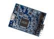
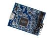
NXP Semiconductors LPCXpresso55S16 Development Board (LPC55S16-EVK)
Ideal platform for evaluation of the LPC551x/S1x MCU family based on Arm® Cortex®-M33 architecture.
NXP Semiconductors MCU-Link Pro SWD Debug Probe
Feature-rich, low-cost debug tool for Arm® Cortex®-M based microcontrollers.
NXP Semiconductors MCU-Link Debug Probe
Powerful board that can be used with MCUXpresso IDE and is compatible with third-party IDEs.

NXP Semiconductors FRDM-MCXE247 Development Board
Design and evaluation platform based on the NXP MCXE247 microcontroller (MCU).
Related Products
NXP Semiconductors LPC5500系列Arm® Cortex®-M33微控制器
基於Arm Cortex-M33的MCU以功率高效的內核提供進階安全性和效能。
NXP Semiconductors LPC55S2x/LPC552x Arm® Cortex®-M33 Microcontrollers
MCUs offering a perfect balance between security, performance efficiency, and system integration.

NXP Semiconductors LPC55S6x Arm® Cortex®-M33 Microcontrollers
Arm® Cortex®-M33-based Microcontrollers combine high integration, security, and power consumption.
NXP Semiconductors PCF85263A Real-Time Clock (RTC) & Calendar
Optimized for low power consumption and with automatic switching to battery on main power loss.
NXP Semiconductors EdgeLock™ SE050 Plug & Trust安全元件系列
交鑰匙安全元件解決方案,為物聯網應用在IC級別提供信任根。
NXP Semiconductors NT3H2x11 NTAG I2C + Connected NFC TAG解決方案
一個被動NFC介面和接觸式I²C介面,專為消費者自動化家居而設計。

NXP Semiconductors NX3DV/NX3L類比開關
類比開關提供寬廣的電源範圍和極低的導通電阻。
NXP Semiconductors NX3L類比開關IC
適用於汽車應用的低電阻開關。
NXP Semiconductors PN7150 Radio-Frequency Identification Transponder
Solution designed to rapidly integrate Near-Field Communication (NFC) technology in any application.

NXP Semiconductors LPC550x/S0x Microcontrollers
Offers advanced security, ideal for industrial, IoT, and general embedded applications.