Nisshinbo RP109x LDO Voltage Regulators
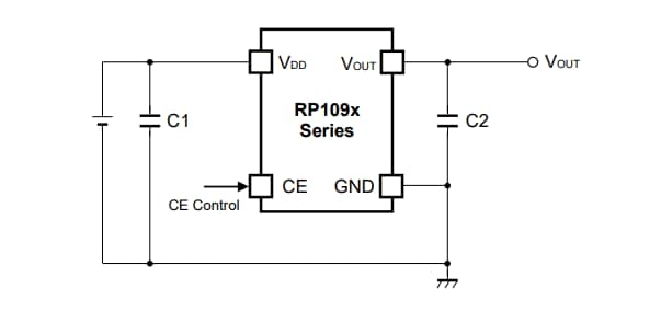
Nisshinbo RP109x LDO Voltage Regulators are CMOS-based voltage regulator ICs featuring high output voltage accuracy, extremely low supply current, low ON-resistance, and high ripple rejection. The RP109x contains a voltage reference unit, an error amplifier, a resistor net for voltage setting, a current limit circuit, and a chip enable circuit.The Nisshinbo RP109x LDO voltage regulators operate with low dropout voltage and a chip enable function, which prolongs the battery life. The line transient response and load transient response of the devices allow for the power supply of hand-held communication equipment. The device has a 0.1µF ceramic capacitor which contributes to the downsizing of hand-held equipment.
The RP109x is available in SOT-23-5, SC-88A, DFN1010-4, and a 0.8mm square ultra compact DFN(PLP)0808-4 package.
Features
- Supply current of 50µA typical
- Standby mode of 0.1µA typical
- Dropout voltage of 0.25V typical (IOUT=150mA, VOUT=2.5V)
- Output voltage accuracy of ±1.0%
- Ripple rejection of 75dB typical (f=1kHz, VOUT=2.5V)
- Temperature-drift coefficient of output voltage
- ±100ppm/°C typical (VOUT<1.8V)
- ±30ppm/°C typical (VOUT≥1.8V)
- Line regulation of 0.02%/V typical
- DFN(PLP)0808-4, DFN1010-4, SC-88A, and SOT-23-5 packages
- 1.4V to 5.25V input voltage range
- 0.8V to 3.6V (0.1V steps) output voltage range
- Built-in fold-back protection circuit of 40mA typical (current at short mode)
- 0.1µF or more ceramic capacitors are recommended to be used with this IC
Applications
- Power source for portable communication equipment
- Power source for electrical appliances such as cameras, VCRs, and camcorders
- Power source for battery-powered equipment
- Power source for home appliances
Block Diagrams

TYPICAL APPLICATION

發佈日期: 2023-02-02
| 更新日期: 2023-02-14


