Diodes Incorporated PI6CG33x Gen 4/5 Compliant Clock Generators
Diodes Incorporated PI6CG33x Gen 4/5 Compliant Clock Generators offer an ideal clock solution for data centers, servers, storage, and network applications using the PCIe interface. The PI6CG33x Clock Generator series includes 2-output, 4-output, 6-output, and 8-output devices. These devices use either a 25MHz crystal or a CMOS reference as an input to generate the 100MHz low-power differential High-Speed Current Steering Logic (HCSL) outputs with on-chip terminations. The on-chip termination eliminates the need for external resistors, simplifies PCB layout, and reduces the cost of materials (BOM). An additional buffered reference output is provided as a low-noise reference for other circuitry.The PI6CG33x Clock Generators use a proprietary PLL design to achieve very low jitter that meets PCIe Gen1/Gen2/Gen3/Gen4/Gen5 requirements. These devices also support Ethernet applications with 50MHz, 125MHz, and 133.33MHz via SMBus. Offering a programmable slew rate and output amplitude for each output, the PI6CG33x Clock Generators provide flexibility for ease of board design and optimal performance. These devices also support selectable spread-spectrum options to reduce EMI for various applications.
The PI6CG33x Clock Generators are in compact, Pb-free, and RoHS-compliant Thin Quad Flat No-Lead (TQFN) packages.
Features
- 3.3V supply voltage
- 25MHz crystal/CMOS input
- 2, 4, 6, or 8 differential low-power HCSL outputs with on-chip termination
- 85Ω or 100Ω output impedance
- Reference CMOS output
- Programmable slew rate and output amplitude for each output
- Differential outputs are blocked until the PLL is locked
- Selectable 0%, -0.25%, or -0.5% spread on differential outputs
- Strapping pins or SMBus for configuration
- Differential output-to-output skew <50ps
- -40°C to +85°C operating temperature range
- Very-low jitter outputs
- <0.3ps RMS, SSC off
- <1.5ps RMS, SSC on
- Differential cycle-to-cycle jitter <50ps
- PCIe Gen1/Gen2/Gen3/Gen4/Gen5 compliant
- CMOS refout phase jitter
- Package options
- TQFN-24 (4mm x 4mm)
- TQFN-32 (5mm x 5mm)
- TQFN-40 (5mm x 5mm)
- TQFN-48 (6mm x 6mm)
- Lead-free and fully RoHS compliant
- Halogen and antimony-free; "Green" device
Applications
- Data centers and servers
- Storage
- Networking systems
- Switches and routers
Datasheets
- 2-Output
- 6-Output
- 4-Output
- 8-Output
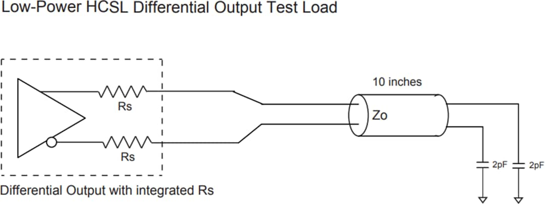
Low-Power HCSL Test Circuit

CMOS REF Test Circuit

Differential Output Driving LVDS

發佈日期: 2020-02-10
| 更新日期: 2024-07-25


