


Altera MAX® 10 FPGA
Altera MAX ® 10 FPGA是一種適用於多種應用的經濟高效、單晶片、非易失性可編程邏輯元件(PLD)。 Altera MAX 10 FPGA具有雙重配置閃存記憶體、用户閃存記憶體、即時啟動功能、整合式模擬數碼轉換器 (ADC),並支援單晶片Nios II軟核心處理器。 這些元件非常適合系統管理、I/O擴展和通訊控制,是工業、汽車和消費應用的理想選擇。
Instant-On, Embedded Dual Image Flash + Extra User Flash:
The MAX® 10 FPGAs include an integrated flash for self-configuring instant-on with dual image support to simplify the board design and save board space. Alternatively, can use the extra flash to store infrequent data logging or processor program code.
Single Power Supply Option:
The single-supply voltage operation makes this suitable for supervisory functions that need to be functional first before all the other system voltage rails have been enabled.
AI-capable DSP blocks:
These devices feature up to 144 embedded multiplier blocks, enabling performance/watt-efficient AI and edge computing solutions. Each block supports 18 x 18-bit or dual 9 x 9-bit multipliers, delivering the computational power needed for demanding AI tasks. These AI tasks include AI-assisted real-time signal processing, video analytics, and sensor fusion.
Integrated Dual Analog to Digital Converter:
The MAX 10 FPGAs consists of up to two built-in analog-to-digital converters with multichannel selection for monitoring power supplies or analog sensors.
Package Options:
The MAX 10 FPGAs contain a wide array of packages from tiny 3x3mm2 chip-scale packages to BGAs with 500 I/O and Quad-Flat Pack (QFP).
特點
- 55nm台積電嵌入式閃存記憶體(Flash+SRAM)制程技術
- 封装
- 低成本、小尺寸封裝 - 支援多種封裝技術和引腳間距
- 具有相容封裝尺寸的多種裝置密度,可在不同元件密度之間無縫遷移
- RoHS6-compliant
- 核心架構
- 4輸入查找表(LUT)和單一暫存器邏輯元件(LE)
- LE排列在邏輯陣列區塊(LAB)中
- 嵌入式RAM和用户閃存記憶體
- 時脈和鎖相環
- 嵌入式乘法器區塊
- 通用I/O
- 內部記憶體區塊
- M9K - 9Kb記憶體區塊
- 用於建立RAM、雙埠和FIFO功能的級聯區塊
- 用户閃存記憶體 - UFM
- 用户可存取的非易失性儲存
- 高速操作頻率
- 大記憶體容量
- 高數據保留
- 多種介面選擇
- 嵌入式乘法器區塊
- 一個18×18或兩個9×9乘法器模式
- 可級聯塊支援建立濾波器、算術函數和影像處理管道
- 模擬數碼轉換器
- 12位元逐次逼近暫存器(SAR)型
- 多達17個模擬輸入
- 累積速度高達每秒100萬個樣本(MSPS)
- 整合式溫度感應功能
- 時脈網絡
- 全球時脈支援
- 時脈網絡中的高速頻率
- 內置內部環形振盪器
- 鎖相環
- 基於模擬
- 低抖動
- 高精度時脈合成
- 時脈延遲補償
- 零延遲緩衝
- 多個輸出抽頭
- 通用I/O (GPIO)
- 多種I/O標準支援
- 片上終止(OCT)
- 最多720Mbps LVDS接收器和發送器
- 外部記憶體介面(EMIF)
- 最多支援600Mbps外部記憶體介面
- DDR3、DDR3L、DDR2、LPDDR2(在10M16、10M25、10M40和10M50上)
- SRAM(僅硬件支援)
- 對於600Mbps性能,需要-6裝置速度等級
- 配置
- 內部配置
- JTAG
- 進階加密標準(AES) 128位元加密和壓縮選項
- 閃存記憶體數據在+85°C保留20年
- 靈活的供電方案
- 單電源和雙電源裝置選項
- 動態控制輸入緩衝器斷電
- 用於動態降低功耗的睡眠模式
應用
- 工業和汽車
- 驅動器、光伏逆變器、電機控制和感應器I/F
- I/O模組、監控與機械視覺
- 驅動器輔助(ADAS)、電動車、ECU和資訊娛樂
- 有線/無線通訊
- I/O擴展和黏合
- 底盤控制
- 消費電子
- 顯示器
- 便擕式、數碼相機和遊戲
- 電腦和儲存
- 伺服器板底盤控制
- 多功能打印機
- 廣播
- 軍事
相關產品

Altera Enpirion® Power Solutions
High-frequency, high-efficiency power management devices for FPGAs, SoCs, CPUs, and ASICs.
視頻監控、視頻門鈴及低功率攝像機

Altera Quartus® Prime Design Software
Multi-platform design environment for all phases of FPGA and CPLD design.
Altera MAX® 10 FPGA Evaluation Boards
General-purpose development platforms for applications like industrial and automotive.

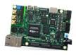
Terasic Technologies DE10-Lite Board
A robust hardware design platform built around the Altera MAX 10 Field-Programmable Gate Array.
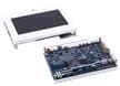
Terasic Technologies MAX 10 NEEK Evaluation Kit
A comprehensive design environment for Altera Max10 FPGAs with included LCD touch panel.
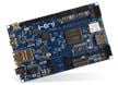
Alorium Technology Hinj Kit IoT & FPGA Development Solution
Features integrated connectivity with built-in driver support and programmable with Arduino.
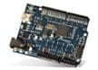
Alorium Technology XLR8 Development Board
Arduino-compatible board that can be used as a drop-in replacement for the Arduino Uno.
Logic Elements
