

 香港
香港


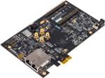
LFE5UM5G-45F-VERSA-EVN

影像僅供參考
請參閱產品規格
請參閱產品規格
842-LE5UM5G45FEVN
LFE5UM5G-45F-VERSA-EVN
製造商:
說明:
可編程邏輯 IC 開發工具 ECP5-5G DEV KIT ECP5 CONN PLATFORM
可編程邏輯 IC 開發工具 ECP5-5G DEV KIT ECP5 CONN PLATFORM
供貨情況
-
庫存:
-
0發生意外錯誤了。請稍後再試。
-
在途量:
-
4預期20/3/2026
-
工廠前置作業時間:
-
2週 工廠預計生產時間數量大於所顯示的數量。
此產品免費航運
Pricing (HKD)
| 數量 | 單價 |
總價
|
|---|---|---|
| HK$3,440.65 | HK$3,440.65 |
- CNHTS:
- 8543909000
- CAHTS:
- 8473302000
- USHTS:
- 8473301180
- TARIC:
- 8523499000
- MXHTS:
- 8473300401
- ECCN:
- 4A994.i
